CBIC imposes ADD on Printed Circuit Boards (PCB) imported from China PR and Hong Kong:
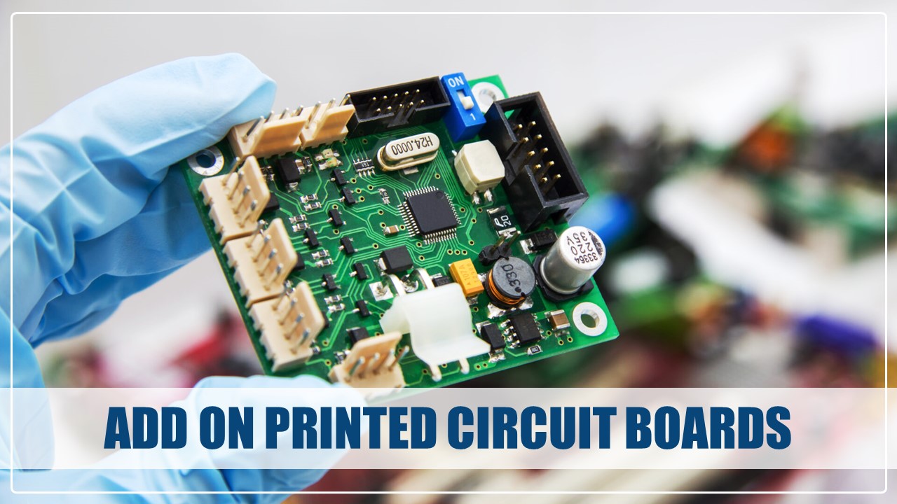
CBIC has notified the imposition of ADD on Printed Circuit Boards (PCB) imported from China PR and Hong Kong via issuing a Notification.
ADD on Printed Circuit Boards
(i) the subject goods have been exported to India from the subject countries below normal values;
(ii) the domestic industry has suffered material injury on account of subject imports from subject countries;
(iii) the material injury has been caused by the dumped imports of subject goods from the subject countries,

and has recommended imposition of an anti-dumping duty on the imports of subject goods, originating in, or exported from the subject countries and imported into India, in order to remove injury to the domestic industry.
Now, therefore, in exercise of the powers conferred by sub-sections (1) and (5) of section 9A of the Customs Tariff Act read with rules 18 and 20 of the Customs Tariff (Identification, Assessment and Collection of Anti-dumping Duty on Dumped Articles and for Determination of Injury) Rules, 1995, the Central Government, after considering the aforesaid final findings of the designated authority, hereby imposes on the subject goods, the description of which is specified in column (3) of the Table below, falling under sub heading or tariff item of the First Schedule to the Customs Tariff Act as specified in the corresponding entries in column (2), originating in the countries as specified in the corresponding entries in column (4), exported from the countries as specified in the corresponding entries in column (5), produced by the producers as specified in the corresponding entries in column (6), and imported into India, an anti-dumping duty as a percentage of the CIF value of the subject goods as specified in the corresponding entries in column (7), of the said Table, namely:-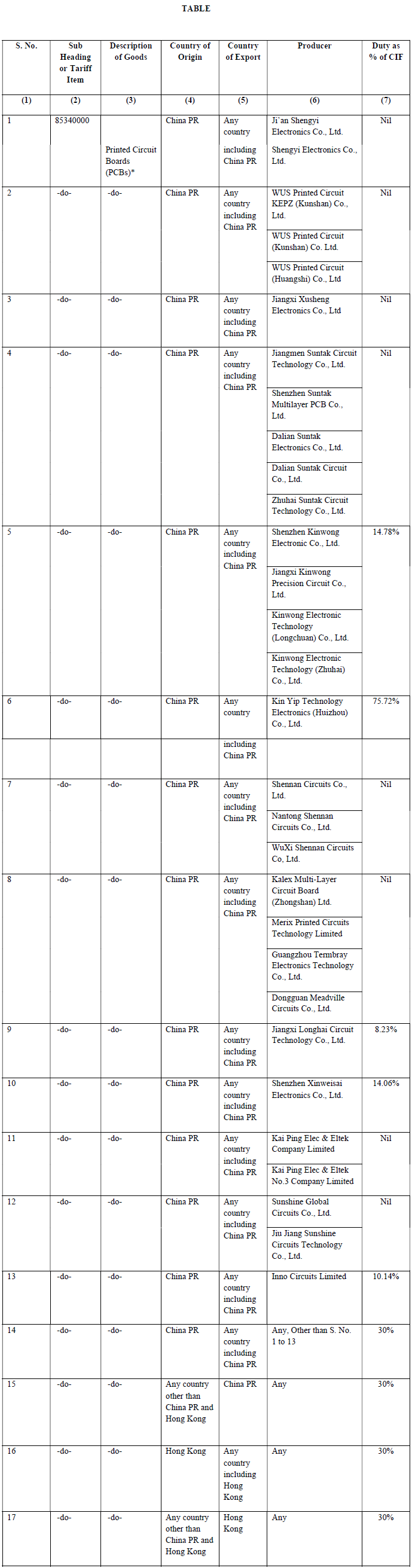
* The following PCBs are excluded from the scope of the product under consideration: -
i. PCBs with more than 6 layers

ii. PCBs for use in mobile phone applications
iii. Populated printed circuit boards of all sizes
iv. PCBs with embedded copper coin
PCBs with embedded copper coin are those PCBs where a metal block is embedded in the middle of the boards. PCBs with embedded copper coin are mainly used for high powered devices requiring high heat dissipation such as base station amplifier products.
v. Inlay PCB
Inlay PCBs are those where copper, aluminium or other material is inlaid or pressed into the printed circuit board and serves to dissipate the heat of an electronic component through the printed circuit board to a bottom side heat sink. The heat-emitting component (heat source) can be connected directly to the metal inlay. Inlay PCBs are mainly used for high-frequency and high-speed products.
vi. Plated Over Filled Via (POFV) PCB or Via-in-Pad PCB
POFV products are designed to save space by putting the conductive holes into the SMD (Surface Mounted Components) pads to be soldered. In order to avoid subsequent soldering paste flowing into the holes and causing false soldering, the holes need to be filled with resin in advance. Afterwards, the surface is plated flat so that the surface of the pads with holes is smooth and does not affect the soldering. In POFV PCBs, the surface is plated with copper. POFV PCBs are mainly used in products with high reliability requirements like wireless base station products, switches, and routers.
vii. High Density Interconnect (HDI) PCB
HDI PCB are those wherein holes are drilled through laser technology with holes size of ≤ 0.1mm. Drilling such small holes needs laser drilling. This is a technology with high processing severity. HDI PCBs are mainly used for high-density products like mobile phones, switches, and servers.
viii. Rigid-flex PCBs
Rigid-flex PCBs are the combination of flexible circuit boards and rigid circuit boards. Rigid-flex PCBs accommodate the good properties of both flexible boards and rigid boards. Rigid-flex products are mainly used in mobile phones, automobiles, industrial control and other applications where there is limited space for electronic parts installation.
ix. Packaging substrates / IC packaging
Packaging substrates or Integrated circuit (IC) substrate is a baseboard used for packaging of bare integrated circuit (semi-conductor) chips. They play a crucial role in connecting the PCB to the semiconductor chip. IC Substrate serves to capture the semiconductor chip, routing to link the chip with the PCB, and safeguard, support, and reinforce the IC chip, thereby giving it a thermal dissipation tunnel.
The anti-dumping duty imposed under this notification shall be effective for a period of five years (unless revoked, superseded or amended earlier) from the date of publication of this notification in the Official Gazette, and shall be payable in Indian currency. Explanation. - For the purposes of this notification, rate of exchange applicable for the purposes of calculation of such anti-dumping duty shall be the rate which is specified in the notification of the Government of India, Ministry of Finance (Department of Revenue), issued from time to time, in exercise of the powers conferred by section 14 of the Customs Act, 1962 (52 of 1962), and the relevant date for the determination of the rate of exchange shall be the date of presentation of the bill of entry under section 46 of the said Act. For Official Notification Download PDF Given Below:About Author

Reetu
Content Manager
 Studycafe
 Delhi, Delhi, India
 8072
8072My Recent Articles
- Income Tax Guide for Indian Defence Personnel for Tax Filing, Taxable Allowances and Other Benefits
- Income Tax Return Breaking: ITR Forms released for AY 25-26
- Ex-DRT Officials Sentenced to 5 Years Rigorous Imprisonment by Madras High Court along with Rs.27 Lakh Fine
- GSTN issued Advisory on Case Sensitivity in IRN Generation
- RBI to issue Notes of Rs.10 and Rs.500 bearing Signature of Guv Malhotra
Loading suggestions…


Recent Posts


All Posts


Tags
Recent Posts
All Posts